- 您现在的位置:买卖IC网 > Sheet目录2000 > IDT82V3155PVG (IDT, Integrated Device Technology Inc)IC PLL WAN T1/E1/OC3 DUAL 56SSOP
Functional Description
16
February 20, 2009
IDT82V3155
ENHANCED T1/E1/OC3 WAN PLL WITH DUAL REFERENCE INPUTS
2.8
OSC
The IDT82V3155 can use a clock as the master timing source. In the
Freerun mode, the frequency tolerance of the clock outputs is identical
to that of the source at the OSCi pin. For applications not requiring an
accurate Freerun mode, the tolerance of the master timing source may
be ±100 ppm. For applications requiring an accurate Freerun mode,
such as AT&T TR62411, the tolerance of the master timing source must
be no greater than ±32 ppm.
The desired capture range should be taken into consideration when
determining the accuracy of the master timing source. The sum of the
accuracy of the master timing source and the capture range of the
IDT82V3155 will always equal 230 ppm. For example, if the master
timing source is 100 ppm, the capture range will be 130 ppm.
2.8.1
CLOCK OSCILLATOR
When selecting a Clock Oscillator, numerous parameters must be
considered. This includes absolute frequency, frequency change over
temperature, output rise and fall times, output levels and duty cycle.
For applications requiring ±32 ppm clock accuracy, the following
clock oscillator module may be used.
FOX F7C-2E3-20.0 MHz
Frequency:
20.0 MHz
Tolerance:
25 ppm 0
°C to 70°C
Rise & Fall Time:10 ns (0.33 V, 2.97 V, 15 pF)
Duty Cycle:
40% to 60%
For Stratum 3 application, the clock oscillator should meet the
following requirements:
Frequency:
20.0 MHz
Tolerance:
±4.6 ppm over 20 years life time
Drift:
±0.04 ppm per day @ constant temperature
±0.3 ppm over temperature range of 0 to 70
°C
The output clock should be connected directly (not AC coupled) to
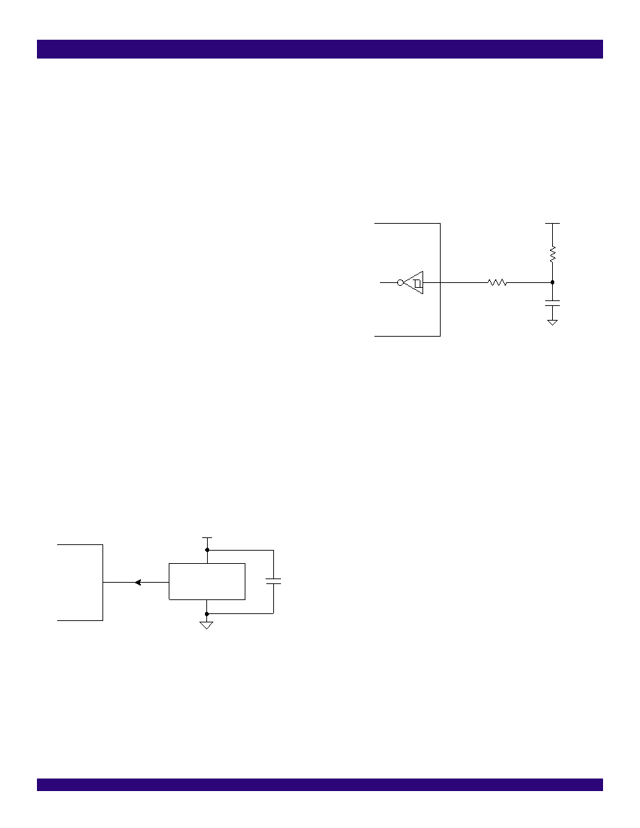
the OSCi input of the IDT82V3155, as shown in Figure - 8.
Figure - 8 Clock Oscillator Circuit
2.9
JTAG
The IDT82V3155 supports IEEE 1149.1 JTAG Scan.
2.10
RESET CIRCUIT
A simple power-up reset circuit is shown as Figure - 9. The logic low
reset pulse is about 50 s.
The resistor Rp is used for protection only and limits current into the
RST pin during power down conditions. The logic low reset pulse width
is not critical but should be greater than 300 ns.
Figure - 9 Power-Up Reset Circuit
+3.3 V
20 MHz OUT
GND
+3.3 V
OSCi
IDT82V3155
0.1
F
3.3 V
R
10 k
Rp
1 k
C
1
F
RST
IDT82V3155
发布紧急采购,3分钟左右您将得到回复。
相关PDF资料
IDT82V3202NLG
IC PLL WAN EBU SGL 68-VFQFPN
IDT82V3255TFG
IC PLL WAN SMC STRATUM 3 64-TQFP
IDT82V3280APFG
IC PLL WAN SE STRATUM 2 100TQFP
IDT82V3285AEQG
IC PLL WAN SE STRATUM 100TQFP
IDT82V3285EQG
IC PLL WAN SE STRATUM 100TQFP
IDT82V3288BCG
IC PLL WAN 3E STRATUM 2 208CABGA
IDT82V3355EDG
IC PLL WAN SYNC ETHERNET 64TQFP
IDT82V3358EDG
IC PLL WAN SYNC ETHERNET 64TQFP
相关代理商/技术参数
IDT82V3155PVG8
功能描述:IC PLL WAN T1/E1/OC3 DUAL 56SSOP RoHS:是 类别:集成电路 (IC) >> 时钟/计时 - 专用 系列:- 标准包装:1,500 系列:- 类型:时钟缓冲器/驱动器 PLL:是 主要目的:- 输入:- 输出:- 电路数:- 比率 - 输入:输出:- 差分 - 输入:输出:- 频率 - 最大:- 电源电压:3.3V 工作温度:0°C ~ 70°C 安装类型:表面贴装 封装/外壳:28-SSOP(0.209",5.30mm 宽) 供应商设备封装:28-SSOP 包装:带卷 (TR) 其它名称:93786AFT
IDT82V3202
制造商:IDT 制造商全称:Integrated Device Technology 功能描述:EBU WAN PLL
IDT82V32021
制造商:IDT 制造商全称:Integrated Device Technology 功能描述:EBU WAN PLL
IDT82V32021NLBLANK
制造商:IDT 制造商全称:Integrated Device Technology 功能描述:EBU WAN PLL
IDT82V32021NLGBLANK
制造商:IDT 制造商全称:Integrated Device Technology 功能描述:EBU WAN PLL
IDT82V3202EDGBLANK
制造商:IDT 制造商全称:Integrated Device Technology 功能描述:EBU WAN PLL
IDT82V3202NLBLANK
制造商:IDT 制造商全称:Integrated Device Technology 功能描述:EBU WAN PLL
IDT82V3202NLG
功能描述:IC PLL WAN EBU SGL 68-VFQFPN RoHS:是 类别:集成电路 (IC) >> 时钟/计时 - 专用 系列:- 标准包装:1,500 系列:- 类型:时钟缓冲器/驱动器 PLL:是 主要目的:- 输入:- 输出:- 电路数:- 比率 - 输入:输出:- 差分 - 输入:输出:- 频率 - 最大:- 电源电压:3.3V 工作温度:0°C ~ 70°C 安装类型:表面贴装 封装/外壳:28-SSOP(0.209",5.30mm 宽) 供应商设备封装:28-SSOP 包装:带卷 (TR) 其它名称:93786AFT